Thursday, 11 June 2020

PARABOLIC DISH STIRLING ENGINE SYSTEM

✏️PARABOLIC DISH STIRLING ENGINE SYSTEM

✏️The collector consists  of  two  axis  tracking. 
✏️Parabolic dish  reflector that  focuses  incoming  sunlight onto a engine/generator. 
✏️The engine uses stirling thermodynamic cycle  to produce  electricity without producing steam as  intermediate step ✏️The dish reflector moves continuously face  towards the sun. 
✏️It  produces  3  to  25kw  per  each  engine. 

 ADVANTAGES: 
1.  Reflecting  surfaces require less  material and  are  structurally simpler than  flat  plate collectors.  (less  cost  ). 
2.  The absorber area of a  concentrating system is  smaller than that of  a  flat plate  system for  same solar  energy collection. 
3.  Loss  of  energy  after collecting  is  less  than  FPC,  because of  large  absorber area in  FPC, working fluid can  attain  higher temperature. 
4.  Owing to the  small area of  absorber per  unit  of  solar energy collecting  area, selective  surface  treatment and/or  vacuum  insulation to  reduce  heat  losses  and improve collector efficiency are  economically feasible. 
5.  Can  be  used for electricity power generation. 
6.  Heat storage  costs  are  less. 
7.  Little  or  no anti  freeze is  required to protect  the  absorber.
 8.  It  is  possible  to get  higher  efficiencies. 

DISADVANTAGES :
1.  Only  beam component is  collected.
 2.  Costly  oriented  systems. 
3.  Additional requirements of  maintenance is  required. 
4.  Non  uniform flux  on  the  absorber. 
5.  Additional optical  losses  such  as  reflectance loss  and  the  intercept  loss, so they introduce  additional factors in  energy  balances. 
6.  High Initial  cost.

DEMAND SIDE MANAGEMENT

✏️TARIFF OPTIONS FOR  DSM

 📌Efficient  use  of resource.
 📌Reduce  average  cost  of electric  power.
 📌Lead to a  reduction  in  need  peaking capacity  and  higher  utilization  of generating power. 
📌A  proper  tariff  itself lead to peak  clipping  and  valley  filling.
 📌Each consumer  should  be charged  equitably  for its  contribution   to the  total costs  for  generation,  transmission  and  distribution  of electric power.

The tariff structures  which  can  promote  DSM  activities  are as  under :

a. Time  of Day  Tariff  (ToD tariff): 
📌It is also  known  as Time of  Use Tariff.  📌Tod  rates make  electricity more  expensive  when  it costs  more  to generate additional  electricity. 
📌It will encourage customer  to shift  their  load  whenever possible  from peak to off peak  thus  flattering  the load  curve.
📌 This  would  be  favourable  to customer  be  seeing the  reduced  bill.
📌 It is also  favourable  to electricity  utility  who  would  gain  by  decreased in  peak  load. 
📌ToD  electricity  meters have inbuilt  timing  unit. 

b) Seasonal  Tariff: 
📌Rate changes  across  the  season. 
📌It is economical  way of managing Demand. 
📌This  type  of tariff does  not  require  special type meters. 
📌Electricity  billing  frequency  has  to be  synchronized  with  time  when seasonal  rates come into  effect.

c)  Curtailable/Interruptible  (C/I)  rates: 📌These rates were suitable  only  for industrial  and  commercial consumers. 📌C/I rates offers incentives  to those  consumers  who reduce  demand  to a  predetermined  level,  when they  receive a notice  to this  effect from the utility. 
📌Success  depends  on  reliable communication  system.


✏️CUSTOMER ACCEPTANCE

📌Customer  satisfaction  should  be  an  index  for measuring  success  of DSM program. 
📌The utility  must  put  great  emphasis  on identifying  and  resolving  the problems  faced  by  customers. 
📌Customer  acceptance  means  willingness  of customer  to participate  in and  adopt  the programme initiated  by the  utility.


The factors  which influence  customer  participation  are: 

a)Incentives: Some programmes  offer specific  incentives  to the customers  to participate in  DSM  activities.  In Tod  tariff  the customers  save on  their  bills  by  shifting  energy usage. 
b) Marketing: Many  approaches   can  be used  to attract customers  to DSM  activities.  Door  to door  campaigns,  media  campaigns  can  help a lot in  this  direction.
 c) Effect  on service: Any  program  which  effects the  desired  energy service  will have effect on  customers  decision  whether  to adopt  the program  or  not.  The aim  should  be  to convince  the  customer  about economical  and  beneficial  for him. 
d) Consumer  Expenditure: High  efficiency equipment  need  more initial  investment.  The  customer  should  be  educated  after  life cycle costs.
 e) Attitude: The energy conservation  program  are more readily accepted and  adopted  than  valley  filling program.  Customers attitudes  can be  altered by  changing  beliefs,  feelings,  self perceptions  and  social  consciousness.


The decision  making process  for adoption  of DSM   program  is more complex  in  case of commercial and  industrial  consumers.  The  reasons are: 

📌The industries  process  required  to be  modified  may be very complex  and  may be  very complex  and  may require  special  design. 
📌The decision  may require  a  hierarchy  if individuals  representing different  functions  in  industrial  and  commercial organization. 
📌The decision  of management  may not  be  acceptable to the  work force.

✏️IMPLEMENTATION ISSUES 

Most  DSM  programs  achieve only  partial  success.  The factors which retain  the  consumers  to move towards energy conservation  are:

📌Lack  of Information :  Consumers  are generally unaware  of the opportunities  of improving  energy efficiency. Energy labels  on equipment's,  devices,  motors  etc  can  be helpful.
📌 Cost  of Energy  Efficient  Equipment: Most  of the customers  are not willing  to purchase  high  efficiency equipment  due  to high  cost. Manufactures  play main  role  in  developing  high  efficiency equipments. 
📌Tariff: In many countries  the tariff for some  categories  of consumers is very low, even lower than  cost  of electricity generation.
 📌Poor  power  Quality  and Reliability: Many equipment  are  sensible to low  voltage and  voltage fluctuation.  Some equipment  consume more power  at  low  voltage.   Power  quality  and  reliability  must  be improved  for  the successive  implementation  of DSM. 
📌Unavailability  of Efficient  Equipments: Many  efficient equipment are not  available in  developing  countries.  The  manufactures  are reluctant  to start  production  of such equipments due to unsure market condition.   Unavailability  of raw materials are also the reason  for this.
📌Small  scale  Sector:   Many equipments are manufactured  in  Small scale industries.   Most  of these  are inefficient.   They produce  low efficient material  in  low cost. 
📌Retirement  of  Inefficient  and  old  Equipment: Most  of  the  time repair  leads  to increasing  inefficient.  They use  substandard equipments in  repair  works 📌Shortage  of skilled  staffs: For identifying, high  skilled  workers  were required. 

DIFFERENT TYPES OF POWER DIODES

✏️Power Diode Types

➡️Depending on the recovery characteristics and manufacturing techniques, thepower diodes can be classified into the following three categories:1. Standard or general-purpose diodes2. Fast-recovery diodes3. Schottky diodesGeneral-purpose diodes are available up to 6000 V, 4500 A, and the rating offast-recovery diodes can go up to 6000 V, 1100 A. The reverse recovery timevaries between 0.1 s and 5 s. The fast-recovery diodes are essential for high-frequency switching of power converters.Schottky diodes have a low on-state voltage and a very small recoverytime, typically in nanoseconds. The leakage current increases with the voltagerating and their ratings are limited to 100 V, 300 A. A diode conducts when itsanodevoltage is higher than that of the cathode; and the forward voltage drop of apowerdiode is very low, typically 0.5 V to 1.2 V.

✏️General-Purpose Diodes

➡️The general-purpose rectifier diodes have relatively high reverse recovery time,typically25 s; and are used in low-speed applications, where recovery time isnot critical(e.g., diode rectifiers and converters for a low-input frequency up to1-kHz applications and line-commutated converters).These diodes cover current ratings from less than 1 A to several thousands ofamperes, with voltage ratings from 50 V to around 5 kV.These diodes are generally manufactured by diffusion.Basically fall into two types.One is called a stud, or stud-mounted type;the other is called a disk,press pak, or hockey-pucktype. In a stud-mounted type,either the anode or thecathode could be the studied. 

✏️Fast-Recovery Diodes

➡️The fast-recovery diodes have low recovery time, normally less than 5 s.They areused in dc–dc and dc–ac converter circuits, where the speed of recovery isoften ofcritical importance. These diodes cover current ratings of voltage from 50 Vto around 3 kV, and from less than 1 A to hundreds of amperes.For voltage ratings above 400 V,fast-recovery diodes are generallymade by diffusion and the recoverytime is controlled by platinum orgold diffusion.For voltage ratings below 400 V,epitaxial diodes provide fasterswitching speeds than those ofdiffused diodes. The epitaxialdiodes have a narrow base width,resulting in a fast recovery time ofas low as 50 ns.

✏️Schottky Diodes

➡️The charge storage problem of a pn-junction can be eliminated (or minimized) in aSchottky diode. It is accomplished by setting up a “barrier potential” with a contactbetween a metal and a semiconductor. A layer of metal is deposited on a thin epitaxiallayer of n-type silicon. The potential barrier simulates the behavior of a pn-junction. Therectifying action depends on the majority carriers only, and as a result there are noexcess minority carriers to recombine. The recovery effect is due solely to the selfcapacitance of the semiconductor junction.The recovered charge of a Schottky diode is much less than that of an equivalent pnjunctiondiode. Because it is due only to the junction capacitance, it is largely independentof the reverse di/dt. A Schottky diode has a relatively low forward voltagedrop.The leakage current of a Schottky diode is higher than that of a pn-junctiondiode. A Schottky diode with relatively low-conduction voltage has relatively highleakage current, and vice versa. As a result, the maximum allowable voltage of thisdiode is generally limited to 100 V. The current ratings of Schottky diodes vary from1 to 400 A. The Schottky diodes are ideal for high-current and low-voltage dc powersupplies. However, these diodes are also used in low-current power supplies for electronic equipments.

✏️Silicon Carbide Diodes

➡️Silicon carbide (SiC) is a new material for power electronics. Its physical propertiesoutperform Si and GaAs by far. For example, the Schottky SiC diodes manufacturedby Infineon Technologies [3] have ultralow power losses and high reliability. They alsohave the following features:• No reverse recovery time;• Ultrafast switching behavior;• No temperature influence on the switching behavior.The typical storage charge QRR  is 21 nC for a 600-V, 6-A diodeand is 23 nC for a 600-V, 10-A device.The low reverse recovery characteristic of SiC diodes, hasalso a low reverse recovery current. It saves energy in manyapplications such as power supplies, solar energy conversion,transportations, and other applications such as weldingequipment and air conditioners. SiC power devices enableincreased efficiency, reduced solution size, higher switchingfrequency, and produce significant less electromagneticinterference (EMI) in a variety of applications.

✏️Silicon Carbide Schottky Diodes

➡️Schottky diodes are used primarily in high frequency and fast-switching applications.Many metals can create a Schottky barrier on either silicon or GaAs semiconductors.A Schottky diode is formed by joining a doped semiconductor region, usually n-type, witha metal such as gold, silver, or platinum.Unlike a pn-junction diode, there is a metal to semiconductor junction.The Schottky diode operates only with majority carriers.There are no minority carriers and thus no reverse leakage current as in pn-junctiondiodes.The metal region is heavily occupied with conduction band electrons, and the n-typesemiconductor region is lightly doped.When forward biased, the higher energy electrons in the n-region are injected into themetal region where they give up their excess energy very rapidly.Since there are no minority carriers, it is a fast switching diode.
➡️The SiC Schottky diodes have the following features:• Lowest switching losses due to low reverse recovery charge;• Fully surge-current stable, high reliability, and ruggedness;• Lower system costs due to reduced cooling requirements;• Higher frequency designs and increased power density solutions.These devices also have low device capacitance that enhances overall system efficiency,especially at higher switching frequencies.

POWER ELECTRONICS BASICS

✏️What is power electronics?
Power electronics is the application of solid-state electronics to the control and conversion of electric power. 

✏️TYPES OF POWER ELECTRONICS CIRCUITS
1. Diode rectifiers
2. Ac–dc converters (controlled rectifiers)
3. Ac–ac converters (ac voltage controllers)
4. Dc–dc converters (dc choppers)
5. Dc–ac converters (inverters)
6. Static switches

1. Diode rectifiers
➡️A diode rectifier circuit converts ac voltage into a fixed dc voltage. 

2. Ac–dc converters (controlled rectifiers)
➡️A single-phase converter with two natural commutatedthyristors is shown in Figure. The average value of the output voltage v 0can be controlled by varying the conduction time of thyristors or firingdelay angle , The input could be a single- or three-phase source. Theseconverters are also known as controlled rectifiers.

3. Ac–ac converters (ac voltage controllers)
 ➡️These converters are used to obtain a variable ac outputvoltage from a fixed ac source and a single-phase converter with a TRIAC isshown in Figure. The output voltage is controlled by varying the conductiontime of a TRIAC or firing delay angle , These types of converters are alsoknown as ac voltage controllers.

4. Dc-dc converters
➡️A dc–dc converter is also known as a chopper, orswitchingregulator, and a transistor chopper is shown in Figure. The averageoutput voltage v 0 is controlled by varying the conduction time t, oftransistor Q1. .If T is the chopping period, then t1 = T.  is called as theduty cycle of the chopper.

5. DC-AC converters
 ➡️A dc–ac converter is also known as an inverter. Asingle phase transistor inverter is shown in Figure. If transistors M1 andM2 and conduct for one half of a period and M3 and M4 conduct for theother half, the output voltage is of the alternating form. The outputvoltage can be controlled by varying the conduction time of transistors

6. static switches
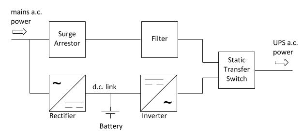
➡️Because the power devices can be operated as static switches orcontactors, the supply to these switches could be either ac or dc and the switches arecalled as ac static switches or dc switches.A number of conversion stages are often cascaded to produce the desired outputas shown in Figure . Mains 1 supplies the normal ac supply to the load through thestatic bypass. The ac–dc converter charges the standby battery from mains. 
2.The dc–ac converter supplies the emergency power to the load through an isolang transformer.Mains 1 and mains 2 are normally connected to the same ac supply.

✏️APPLICATION OF POWER ELECTRONICS

🔋Power electronics have revolutionized the concept of power control for powerconversionand for control of electrical motor drives.Power electronics combine power, electronics, and control.

🔋Control deals with the steady-state and dynamic characteristics of closed-loop systems. 

🔋Power deals with the static and rotating power equipment for the generation,transmission, and distribution of electric energy. 

🔋Electronics deal with the solid-state devices and circuits for signal processing tomeet the desired control objectives.Power electronics may be defined as the applications of solid-state electronics for thecontrol and conversion of electric power.Power electronics are based primarily on the switching of the power semiconductor devices.

MICRO-CONTROLLER BASICS

✏️What is a micro-controller? 
A microcontroller is a small computer on a single metal-oxide-semiconductor integrated circuit chip.
✏️DIFFERENCE BETWEEN MICROCONTROLLER AND MICROPROCESSOR 

✏️FACTORS THAT HAS TO BE REMEMBERED WHILE CHOOSING A MICROCONTROLLER 

1. 8 bit, 16 bit, 32 bit microcontroller (whether we require any 1 one of these)
2. Speed
3. Packaging (either dual in line packaging or quad flat packaging)
4. Power consumption
5. The amount of ram and rom on the chip
6. The number of input output pins and timer on the chip.
7. Cost per unit. 
8. How easily we can upgrade it to higher performance or lower power consumption.
9.The second microcontroller products criterion is how around it. 
10.The third criterion microcontroller needed quantity is its both easy now in it in ready and choosing is to a develop choosing availability in the future a in .

✏️COMPONENTS OF A COMPUTER SYSTEM 

✏️System  Bus 

*Address  Bus:An internal channel from the CPU to memory across which the addresses of data (not the data) are transmitted. The number of lines (wires) in the address bus determines the amount of memory that can be directly addressed as each line carries one bit of the address.

 *Data  Bus: may refer to: Bus (computing), a communication system that transfers data between different components in a computer or between different computers. Memory bus, a bus between the computer and the memory.

* Control  Bus:control bus is part of the system bus, used by CPUs for communicating with other devices within the computer. 

✏️APPLICATIONS OF MICROCONTROLLER 

Microcontrollers are used in automatically controlled products and devices, such as automobile engine control systems, implantable medical devices, remote controls, office machines, appliances, power tools, toys and other embedded systems.

BIOGAS USES AND BENEFITS

✏️What is biogas? 
Biogas is the mixture of gases produced by the breakdown of organic matter in the absence of oxygen (anaerobically), primarily consisting of methane and carbon dioxide. Biogas can be produced from raw materials such as agricultural waste, manure, municipal waste, plant material, sewage, green waste or food waste.

✏️BENEFITS OF BIOGAS

1. Biogas is eco-friendly.
2. It reduces soil and water pollution
3. Biogas generation produces organic fertilizer.
4. It is simple and low cost technology.
5. Healthy cooking alternative for developing areas.


✏️SELECTION OF SITE FOR A BIOGAS PLANT

1.DISTANCE:
The distance between the plant and the site of consumption should be less in order to achieve economy in pumping of gas and minimizing the gas leakage. For a plant of capacity 2 m³,the optimum distance is 10m.
2.OPEN SPACE :
The sunlight should fall on the plant as temperature between 15°c to 30 °c is essential for gas generation at good rate.
3.WATER TABLE:
The plant is normally constructed underground for ease of charging the feed and unloading slurry requires less labour. 
Plant should not be constructed if the water table is more than 3m.
4.SEASONAL RUN OFF:
Proper care has to be taken to prevent the interference of run off water during the monsoon.
5.DISTANCE FROM WELLS:
The seepage of fermented slurry may pollute the well water .Hence minimum of 15m should be maintained from the wells.
6.SPACE REQUIREMENTS:
Sufficient space must be available for day to day operation and maintenance.
7.AVAIALABILITY OF WATER:
Plenty of water must be available the cow dung slurry with a solid concentration of 7% to 9% is used.

floating dome type biogas plant 👆


✏️BIOGAS PLANT FEEDS

1.ANIMAL WASTES:
Cattle dung, goat and poultry droppings, fish wastes, leather and wood wastes ,piggery wastes etc.
2.HUMAN WASTES:
Faeces, urine and other wastes .
3.AGRICULTURAL WASTES:
sugarcane trash, spoiled fodder, cotton and textile wastes etc.
4.WASTE OF AQUATIC ORIGIN:
Marine plants, algae, water weeds etc.
5.INDUSTRIAL WASTES:
Sugar factory, tannery, paper etc.

✏️FUTURE OF BIOGAS PLANT 

In future we are generally adopting renewable energy sources, so we could see a lot of usage of biogas plants. 

Since the food waste, household waste all can be use effectively and use of LPG can be minimized. 

Finally the last product in the digester can be used as fertilzers for plant, which helps the plants to grow in a proper healthier manner. 

SOLAR CELLS

What is solar cell?

A structure that converts solar energy directly to DC electric energy.
It is like a battery because it supplies DC power
It is different from the battery in the sense that the voltage supplied by the cell changes with changes in the resistance of load.

COMPONENTS OF SOLAR CELLS 

These include solar cell panels, one or more batteries, a charge  regulator or controller for a standalone system, an inverter for a utility grid-connected system, requirement of alternating current(AC) rather than direct current(DC), wiring, and mounting hardware or a framework.

KEY ELEMENTS OF SOLAR CELL

SUBSTRATE
It is an unpolished p-type wafer referred to as p-region base material.
The important parameters to be kept in mind while choosing a wafer for solar cells are its orientation, resistivity, thickness and doping.
Typical thickness of wafers used for solar cells is 180-300µm.
The typical resistivity values are in 1-2Ωcm. 
The doping should be close to 5×10^15/〖𝑐𝑚〗^3 to 1×10^16 /〖𝑐𝑚〗^3.
The wafer can be single crystalline or multi crystalline.


EMITTER
The emitter formation involves the doping of silicon with pentavalent impurities such has Ph, Ar and antimony.
However, for solar applications Ph is widely used has impurity.
Doping is done by process of diffusion.
The junction depths are in the range of 0.2- 1µm.
This is also commonly known as n- region diffused layers.


ELECTRICAL CONTACT 

These are essential to a photovoltaic cell since they bridge the connection between semiconductor material and external electrical load.
It includes:
Back contact: It is metallic conductor completely covering back. The back contact of a cell is located on the said away from incoming sun light and is relatively simple. It usually consists of a layer of aluminium.
Front contact: Current collection grid of metallic finger type is arranged in such a way that photon energy fall on N-region diffused layers. The front contact is located on the side facing the light source and is more complicated. When light falls on solar cell a current of electrons flow over the surface.
Anti- reflective coatings: They are applied to reduce surface reflection and maximize cell efficiency in solar glass and silicon solar cell manufacturing. When a thin-film nano-coating anti- reflecting coating of silicon dioxide and titanium dioxide is applied, there seems to be an increase in cell efficiency by 3-4%.

SOLAR CELL MATERIALS 

Many combinations of materials and methods of fabrication of photovoltaic cells are now either in practical use or in various developmental stage.
Silicon is the most widely used basic material because of its suitability and its availability in abundance.
More than 80% are crystalline silicon solar cells.
Other 20% are developed as amorphous silicon solar cells.
The band gap of a semi-conductor material is the minimum energy needed to move an electron from its bound state within an atom to a free state.
The lower energy state is ‘valence band’ and higher is ‘conduction band’ .

SILICON

This remains the most popular material for solar cells, including these types;
Mono crystalline or single crystal silicon
Polycrystalline silicon 
Amorphous silicon 

Polycrystalline wafers are made by a casting process in which molten silicon is poured into a mould and allowed to set.
They are sliced into wafers.
They are significantly cheaper but not efficient.

Amorphous silicon, one of the thin film technologies, is made by depositing silico onto a glass substrate from a reactive gas like silane.
There are many advantages of thin film cells 
Easier deposition and assembly 
Ability to deposited on inexpensive substrates 
Ease of mass production 
Suitability to large applications. 

PRACTICAL SOLAR CELLS

Solar cells are now manufactured from a number of different semiconductors that are summarized in the following points. 
 

Crystalline silicon cells: They dominate the photovoltaic market. To reduce the cost, they are often made from multi-crystalline material, rather then from the more expensive single crystals. The technology is well established. The modules have long life time (20years or more).
Amorphous silicon solar cells: they are cheaper type of silicon cells made in the form of amorphous thin films that are used to power a variety of consumer products; but they are less efficient. 
Cadmium telluride and copper indium diselenide: Thin-film modules are now beginning to appear on the market and hold the promise of combining low cost with acceptable conversion efficiencies.
High efficiency solar cells: From gallium arsenide, indium phosphide or their derivatives are used in specialized applications, for example, to power satellites or in systems that operates under high-intensity concentrated sunlight.   

💁‍♂️ARTIFICIAL SUN CREATED BY CHINA 👈

🌞 ARTIFICIAL SUN MADE BY CHINA 🌞 ☀️China successfully powered up its “artificial sun” nuclear fusion reactor for the first ti...